Research project
The 3IT, Umicore and ESA Research Chair in Semiconductor Nanomembranes and Flexible Optoelectronics is dedicated to advancing the science and technology of next-generation materials for sustainable electronics and energy systems. Its goal is to develop innovative semiconductor nanomembranes and flexible optoelectronic platforms that combine high performance with lightweight, scalable, and energy-efficient designs. By bridging fundamental research with real-world applications, the Chair aims to accelerate the transition toward cleaner energy solutions, smarter devices, and sustainable materials, while fostering collaboration between academia, industry, and society.
3IT
Umicore Inc.
European Space Agency – ESA
3IT, Umicore and ESA Research Chair in Semiconductor Nanomembranes and Flexible Optoelectronics
- Towards flexible electronics
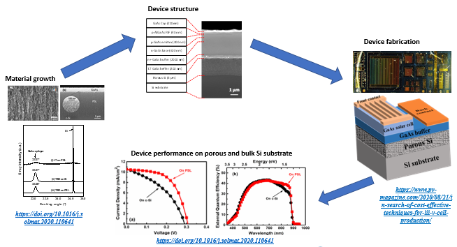
Porous germanium Efficient Epitaxial LayEr Release (PEELER) for low cost high performance III-V solar cells
- The development of an innovative process in the field of solar energy
Graphene-Mesoporous Si Nanocomposite
- 2D Graphene, hybrid heterostructures and advanced In-situ observations
High efficiency III-V Solar cells using a mesoporous Ge separating interface
- III-V solar cells on porous Silicon
- Duplicated-Junction Solar Cells: An Innovative Approach for Energy Harvesting at Ultra-High Concentrations
- Nanostructured Si pillars as a compliant substrate for defect-free heteroepitaxy
Nanovoids and defects in Ge/Si substrate for integration of III-V materials
- Defects in Ge/Si substrate for integration of III-V materials
Annealed porous Si for Li-ion batteries
- On-chip Microbattery for IOT applications
III-V solar cells on porous Silicon
III-V solar cells on porous Silicon
Epitaxial growth of III–V and group IV compounds, followed by the fabrication of optoelectronic devices based on these materials, lies at the core of our research activities. Using advanced deposition techniques, we engineer high-quality crystalline layers with precise control over composition, thickness, and interface properties.
Author : Alex Brice Poungoué Mbeunmi
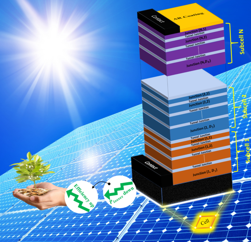
Duplicated-Junction Solar Cells: An Innovative Approach for Energy Harvesting at Ultra-High Concentrations
Duplicated-Junction Solar Cells
New architecture of solar cells called duplicated junction cells. The concept constitutes an innovative alternative to conventional III-V multi-junction cells and consists in duplicating each sub-cell in several p-n junctions of the same material. The architecture makes it possible to considerably reduce resistive losses and therefore to operate efficiently at very high concentration factors (> 1000 suns).
Author : Mohamed El-Gahouchi
2D Graphene, hybrid heterostructures and advanced In-situ observations
2D Graphene, hybrid heterostructures and
This research project explores several key topics, including the growth of monolayer graphene on semiconductor substrates (Ge, GaAs, etc.), wafer-scale single-crystalline 2D graphene (100–300 mm), detachable III–V/IV/graphene heterostructures for optoelectronic and photovoltaic applications.
Author : Thierno Mamoudou Diallo

Graphene-Mesoporous Si Nanocomposite
Graphene-Mesoporous Si Nanocomposite
Silicon and germanium are semiconductors of interest for energy applications. Electrochemical etching allows to nanostructurated semiconductors with nanoscale size and tunable morphology. Chemical vapor infiltration with acetylene and controled steps as well as temperature control conduct to graphene deposition into the mesoporous structure (all the surface is covered). Then advanced material characterizations using Raman, SEM, TEM, XPS for understanding the structure and nature of the deposition are performed. Finally, thermoelectric properties are studied on this new kind of nanomaterial.
Author : Stephanie Sauze
Nanostructured Si pillars as a compliant substrate for defect-free heteroepitaxy
Nanostructured Si pillars as a compliant substrate for defect-free heteroepitaxy
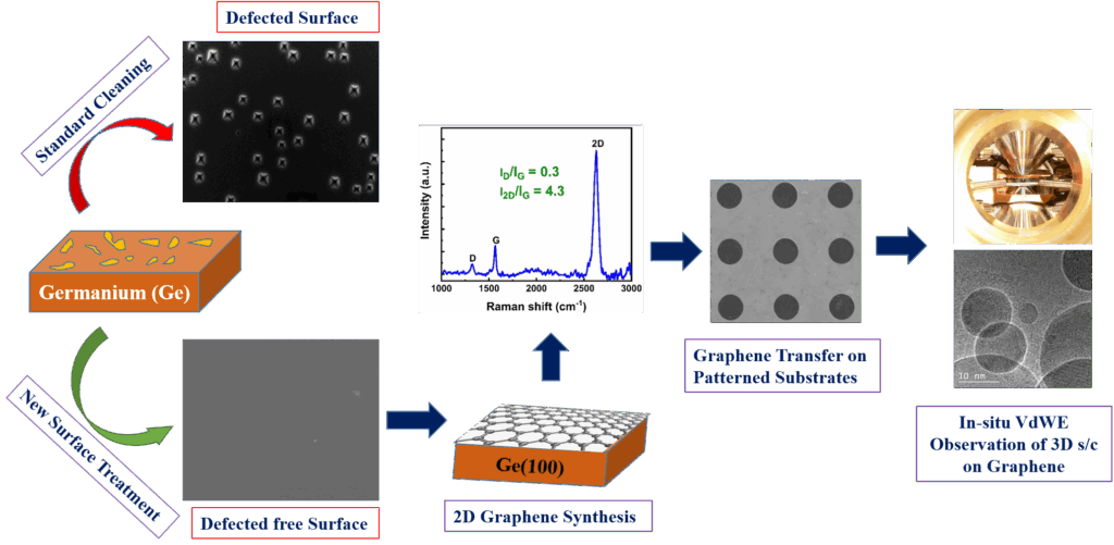
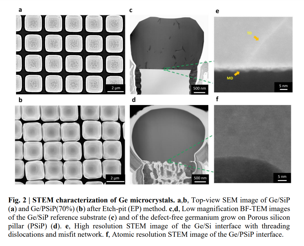
A perfectly compliant substrate would allow the monolithic integration of high-quality semiconductor materials such as Ge and III-V on Silicon (Si) substrate, enabling novel functionalities on the well-established low-cost Si technology platform. Here, we demonstrate a compliant Si substrate allowing defect-free epitaxial growth of lattice mismatched materials. The method is based on the deep patterning of the Si substrate to form micrometer-scale pillars and subsequent electrochemical porosification. The investigation of the epitaxial Ge crystalline quality by X-ray diffraction, transmission electron microscopy and etch-pits counting demonstrates the full elastic relaxation of defect-free microcrystals. The achievement of dislocation free heteroepitaxy relies on the interplay between elastic deformation of the porous micropillars, set under stress by the lattice mismatch between Ge and Si, and on the diffusion of Ge into the mesoporous patterned substrate attenuating the mismatch strain at the Ge/Si interface.
Author : Alexandre Heintz
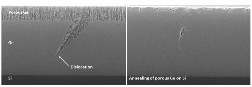
Defects in Ge/Si substrate for integration of III-V materials
Defects in Ge/Si substrate for integration of III-V materials
We use electrochemical etching of Ge/Si substrates to create voids along dislocations, followed by thermal annealing to promote their coalescence. These voids deflect or annihilate dislocations, lowering threading dislocation density to ~10⁴/cm². This method is a promising route for integrating III–V materials on silicon for high-efficiency solar cells.
Author : Jonathan Henriques
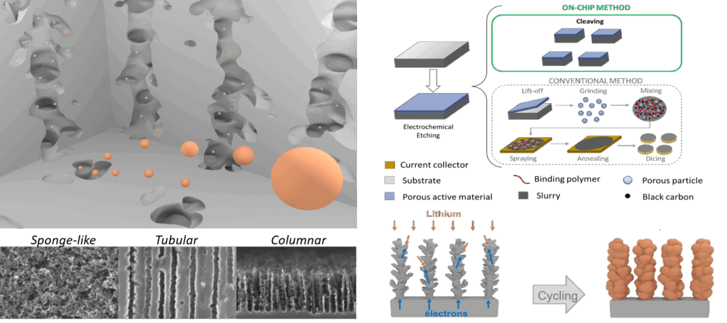
On-chip Microbattery for IOT applications
On-chip Microbattery for IOT applications
High-performance anode materials like silicon and germanium face challenges such as volumetric expansion and solid electrolyte interface (SEI) formation. Nanostructuring improves their lifetime and mechanical stability, while carbon functionalization reduces SEI and irreversible capacity. Building on this, we developed mesoporous germanium–graphene nanocomposites using scalable electrochemical etching and chemical vapor deposition, achieving superior electrochemical performance in both high-energy and high-power applications.
Author : Arthur Dupuy